The progress of nanotechnologies has led to the development of versatile nanostructures with novel functionalities. For example, carbon-based nanostructures such as carbon nanotubes (CNT) and graphene have extraordinary electrical properties with high carrier mobilities and, thus, can be utilized to develop advanced electronic devices overcoming the limitations of conventional devices. As another example, nanoparticles (NPs) have completely different optical properties from conventional materials. Thus, they can be utilized to develop optoelectronic devices with new functions. Further, one can organize different nanostructures to fabricate a ŌĆ£hybrid nanostructureŌĆØ having even more advanced functionalities. One of our research goals is to develop and investigate hybrid nanostructures for advanced electronic and optoelectronic devices.
Surface-Programmed Assembly of Nanowires (Nature Nanotechnology1 66 2006)
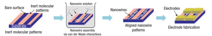
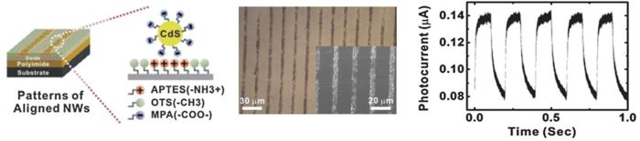
Generally, as grown individual nanostructures such as nanotubes and nanoparticles exist in the form of dried powders or are dispersed in a liquid solution. Thus, one has to assemble and arrange them on a solid substrate in a planned manner, as a first step to build a hybrid nanostructure for a practical application. However, the precise assembly of nanostructures has been very time-consuming and difficult, hindering basic studies and practical applications of the hybrid nanostructures. To solve the problem, we developed a ŌĆ£surface-programmed assemblyŌĆØ method for the efficient large-scale integration of nanostructures via directed-assembly strategies. In the method, inert molecular layers are first patterned on a solid substrate in various ways. Then, nanostructures are absorbed on the bare regions of the substrate via a self- or forced-assembly. For the molecular layer patterning, various processes could be utilized. For an example, a photolithography could be used to fabricate wafer-scale patterns of molecular layers.
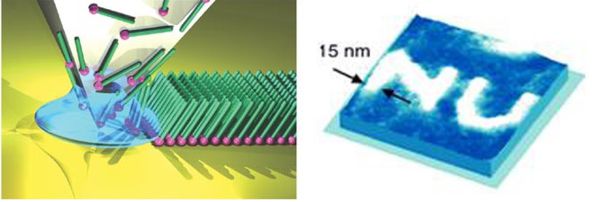
For nanoscale patterning of molecular layers, an advanced nanotechnology such as a dip-pen nanolithography (DPN) could be utilized. DPN utilizes a sharp atomic force microscopy (AFM) tip as a nanoscale pen, organic molecules as ink, and a solid substrate as a paper. When the molecule-coated tip is in contact with the substrate, molecules diffuse out onto the substrate, chemically anchor to the surface, and form well-ordered self-assembled monolayer (SAM) patterns. Using those methods, we can assemble versatile hybrid nanostructures and investigate their unique electrical and optical characteristics.
Following are a few examples of our researches on hybrid nanostructures.
1) Electronic Channels based on Aligned Nanowires
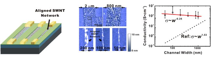
Aligned Networks of Single-walled Carbon Nanotubes (Small5 1642 2009)
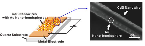
We fabricated 100 nm-scale conducting channels based on ŌĆśalignedŌĆÖ single-walled carbon nanotubes (swCNTs) or cadmium sulfide (CdS) nanowires. Compared with conventional randomly-oriented networks, the aligned nanotube/nanowire networks exhibited a much larger carrier mobility, due to the reduced effective length of current paths and the increased packing density of nanotubes/nanowires in the channels. In addition, by further hybridizing the channels with other nanomaterials, we could develop advanced electronic/optoelectronic devices with enhanced performances.
2) Hybrid Nanostructures for Optoelectronic Devices
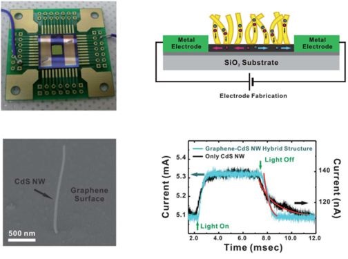
We fabricated the hybrid nanostructure of graphene and CdS nanowires for an optoelectronic application. The hybrid structure was comprised of CdS nanowires which were selectively grown in specific regions on a single-layer graphene. The photoconductive channels based on our grapheneŌĆōCdS nanowires hybrid structures exhibited higher photocurrents as well as a faster operation speed than conventional CdS-nanowire networks. The hybrid nanostructure can be useful for practical applications because they are much faster than commercial CdS film-based photodetectors and exhibit photo responses large enough for practical applications.
3) Nano-Bio Hybrid Structures
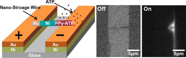
Nano-Storage Wire to Store Biomolecules (ACS Nano7 6906 2013)
Nano-storage wire (NSW) is an example of our nano-bio hybrid structures with novel functions. The NSW is a multi-segmented nanowire composed of a polypyrrole segment containing chemical species such as adenosine triphosphate (ATP), a ferromagnetic nickel segment, and a conductive gold segment. NSW can store desired chemical species and release them at a desired moment via external electrical stimuli. For example, the NSWs could be used to deliver ATPs to motor proteins in nano-bio devices and to control the biomotors. Further, NSWs can be printed onto various substrates, to build versatile chemical storage devices.